
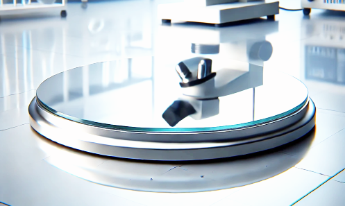
Interferometer for optical 3D measurement
An interferometer for highly accurate detection of surface structures on the micro and nano level is a particular advance in technology. Geometries can be recorded and evaluated in their entirety without contact. The possibility to capture fast and easily the entire geometry of an object is a big step forward compared to two-dimensional measurements.Learn more:

Explanation of the concepts of coherence and interference
Coherence:
The coherence describes the property of a light beam or wave to behave consistently in its shape when moving through space. It is also a condition for the formation of interference. The waves that meet have the same frequency and a constant phase shift to each other.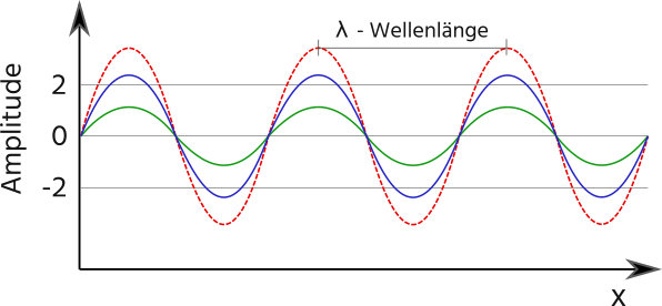
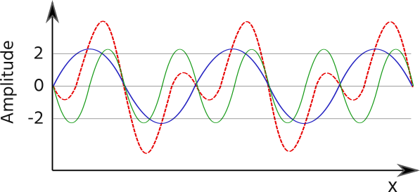
Interference:
Interference is the result of the superposition of coherent waves on each other. Two identical waves meet and cancel or superimpose each other. These two cases are described as destructive and constructive interference.

Interferometer - fast 3D surface measurements with high accuracy
A classical white-light interferometer based on the principle of a Michelson interferometer can be used as a basis for high-precision 3D measurements. In principle, a measuring object is illuminated with coherent light by a light source [1] and the reflecting light of the measuring surface [4] is used for evaluation. A reference mirror [5], which is exposed by the same light beam via a beam splitter [3], helps here. If the measuring surface of a sample is at the same distance from the beam splitter as the reference mirror, then interference of the coherent light beams occurs. Via an optical system, the light is further guided to a camera chip [6] as a detector. The user sees a wave-like pattern in the overview image depending on the surface position. This is the indication that the measuring surface is at the same distance from the known reference path length of the system. This defines the reference plane in which height data of the measurement object can be measured. To measure the three-dimensional shape of a surface, the measuring object moves through this reference plane. In doing so, either the sensor or the sample can position itself in the height.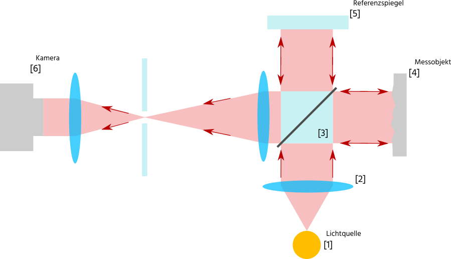
Order measurements:

#1 Optical 3D Measurement
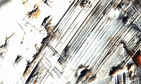
Roughness Measurement
The roughness measurement (surface measurement) is used to determine the surface roughness. For this purpose, a two- or three-dimensional profile of the surface is measured. From this, various roughness parameters are calculated using standardized methods to characterize the surface roughness.
#2 Optical 3D Measurement
Topography Measurements
Capturing surface profiles and structures to create three-dimensional height maps of surfaces. This is crucial for the evaluation of materials such as semiconductors, microchips, and other finely structured components.
#3 Optical 3D Measurement
Flatness Inspection
Flatness testing is a critical process for determining the flatness of surfaces, especially important in the semiconductor industry and the manufacturing of optical components such as lenses and mirrors. Through precise measurement methods, flatness testing enables the identification of irregularities, ensuring the quality and functionality of the products.
#4 Optical 3D Measurement
Abrasion Studies
Wear and abrasion studies are essential procedures for assessing wear on surfaces and materials, caused either by specific tests or long-term use. These analyses are crucial for evaluating the durability and quality of materials or coatings and identifying potential weaknesses.
#5 Optical 3D Measurement
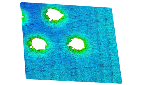
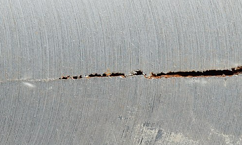
Defect and Failure Analysis
Defect and failure analysis plays a central role in detecting and characterizing microcracks, scratches, particles, or other defects on surfaces that can significantly affect the performance and quality of products. Accurate identification of these flaws is crucial for quality assurance and allows companies to implement targeted corrective actions.